Commercial Computer Vision was changing the game in various parts of our life over the past 2 decades. It has automated manufacturing, increased the yield in agriculture, analyzed sports matches, and secured public spaces and private properties.
Since late, the advent of Deep Learning revolutionized this already revolutionizing technology. Artificial Intelligence-powered Machine Vision leveraged the capability to train brain-inspired artificial neural networks with pre-classified sample images. The algorithms behind are referred to as Deep Learning. With Deep Learning models, a machine can distinguish good from bad objects and normal from unusual appearance. Even challenging tasks can be solved today, from the quality inspection of food to autonomous driving.
The application of a trained Deep Learning model on new images requires inference processing, a quite computationally expensive task. This inference processing can be widely parallelized. Thus, aside from multi-core CPUs, GPUs, and FPGAs, dedicated vision inference processing chips, aka Tensor Processing Units (TPUs) or Vision Processing Units (VPUs), made their way into modern solutions, especially in embedded systems.
In the coming years, the AI hardware market is expected to grow at a CAGR of more than 37%. The market is projected to reach 234.6 billion by 2025 (Source: Tractica).
At the Vision Show in Stuttgart 2018, the first “inference camera” with an embedded Intel Movidius Myriad VPU on board was presented. Since late, powerful low-code and even no-code software solutions became available to manage the whole Deep Learning pipeline from image collection, selection, annotation, training, and deployment. With these enabling ecosystems, numerous OEMs are offering inference cameras with different performance characteristics, today.
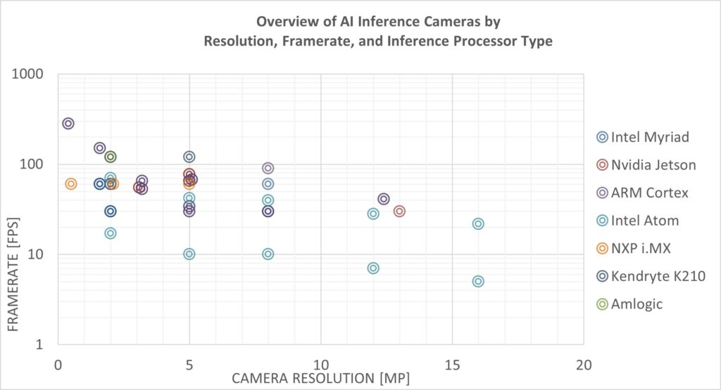
The following chart shows one result of a current market study by Vision Markets of 91 inference cameras from 20 different OEMs. Here, cameras are plotted by their resolution and frame rate while the dot color indicates the type of inference chips.

For illustration purposes, multiple inference chip models have been clustered herein, such as Intel’s Movidius Myriad chips MA2085, MA2450, and MA2485, or Nvidia’s Jetson Nano and Xavier NX, as well as Qualcomm’s QCS605 and QCS603 or NXP’s i.MX RT1064 and i.MX 8M Plus, etc.
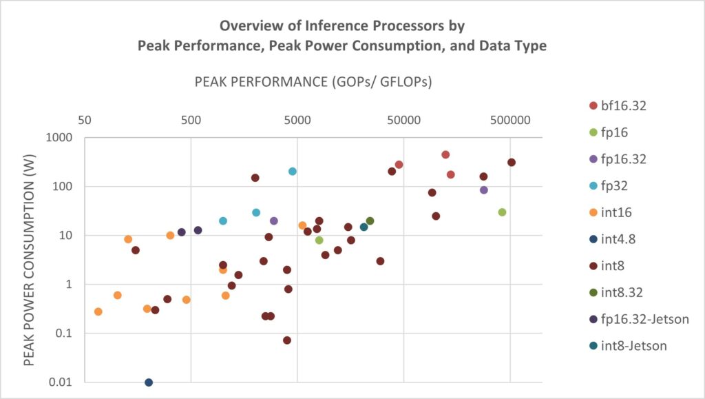
When selecting the inference processing chip for an inference camera, multiple factors come into play: processing speed, power consumption, memory bandwidth and/or applicable model size, and existing ecosystems for the simple deployment of trained models to the camera.
The power consumption of the chip is critical as it defines the minimum size of the camera since power consumption creates heat and heat is harmful to the noise level of the image sensor.
The chart below shows 55 inference processing chips by their peak performance peak power consumption and data type. Besides dedicated chips for embedded systems, the chart also contains models designed for PC processing cards or data centers.

Most cameras that are promoted as inference cameras use embedded chips by Intel, Amlogic, Qualcomm, NXP, or Kendryte as well as CPU/GPU architectures such as ARM Cortex, Nvidia Jetson, and even plain multi-core CPUs like Intel Atom.
Are you interested in AI inference cameras, their market, applications, and providers?
Vision Market’s customers can access:
- Full database of AI inference cameras with ~1400 technical attributes as well as links to product information and supported Deep Learning frameworks
- Company briefs about every OEM providing inference cameras
- Overview of commercial applications of inference cameras
- Individual consulting in the field of Deep Learning, Edge-AI, business models, market potentials, target customers groups, etc.


